![[Previous Page]](dprevpag.gif)
![[Next Page]](nextpage.gif)
![[Up]](up.gif)
![[Home Page]](homepage.gif)
Note: The below abstract is from 2001
Also see:
* Photoplotting / Photomasks - Services
* Photoresists / Phototools
* Gerber Editors / Viewers, Data Conversion & Translation Software
Gerber Data & Photoplotting Related:
* Gerber Format Plot Data Format Reference Book / Gerber Format Specifications
* D-codes, Apertures & Gerber Plot Files under Technical / How to Pages / Hobby - DIY / Technical Bulletins / Tips & Techniques
UNIVERSITY OF HERTFORDSHIRE
Faculty of Engineering and Information Sciences
Department of Manufacturing Systems
A REVIEW OF MODERN PHOTOPLOTTING FORMATS
By Graham Dean
Electronics Manufacturing Technology
Abstract
This paper provides a short summary of some of the formats used in the computer aided design and manufacture of printed circuit boards. Photoplotting and Gerber data formats being the start of this whole process. The fundamentals of photoplotting are explained and the development from the vector Gerber format to the laser photoplotter and is described. The development of up-to-date software and the relative merits of modern formats are discussed.
Acknowledgements
The author would like to express thanks to Martin Phillips of Phillips Precision Photography for allowing the author to visit his premises. Julian Coates, Vice President, Corporate Marketing, Valor Computerised Systems Ltd for his valuable time on the telephone. Danny Carr, President, D03* Inc for his emails and kind offer to publish this paper on the Everything PCB Website.
1. Introduction
With the growing demand for high quality, low cost electrical products, it has become essential for computer-aided tools to be used for the design and fabrication of printed circuit boards (PCB). Most companies have adopted the new electronic design and automation (EDA) systems to produce high quality products, using more economical methods like computer-aided design (CAD) and computer aided manufacture (CAM). The production of PCB’s used to be a very labour intensive and time consuming process, hence there was a requirement to speed things up and shorten the manufacturing time.
The objective of this report is to provide general information on the process of photoplotting and its data formats. The paper is intended to be short and give a basic understanding of the process and analyse the impact of EDA and PCB CAD/CAM. The author has no personal experience, as a user, of any of the formats covered in this paper. All the information has been gained from research and information supplied from knowledgeable and reliable sources. Before we are in a position to look at photoplotting formats, we will have to understand the fundamentals of a photoplotter, how it is controlled, and its role in EDA. No matter how powerful your design software may be, you will eventually create a photoplot file. In this report we will look at this file (called Gerber data) and its progression in PCB CAD/CAM in the development of new, more productive software.
2. METHOD OF INFORMATION COLLECTION
The method chosen to gain information on this technology was to seek reliable information sources from throughout the industry and make contact with the professionals in photoplotting and EDA. Initially, sources of information were found in the University of Hertfordshire library and on the Web. PCB manufacturing methods are continually being developed and so accessing up-to-date material proved difficult. The majority of reference books were published in the mid 1980’s and contained dated photoplotting methods, however they did give good background reading into the history of the process. From Web searches, personal contact was made with individuals by email. By telephone and email, some of the most respected people in the field, from around the world, have supplied very helpful advice and information. Photoplotting bureau’s1 have been visited to see the process in action. The most helpful individuals were emailed questionnaires, to get their personal opinions on the various formats and how they saw the future of photoplotting formats.
3. DEFINITION OF PHOTOPLOTTING
A photoplotter is just what it the name implies: a plotter that writes using light. It uses light to draw accurate lines and shapes on photosensitive medium and replaces what used to be a very time consuming task done by hand. The photoplotter follows data instructions to generate what is called an “artwork”.
4. HISTORICAL DEVELOPMENT
The Gerber Scientific Instrument Company developed a photoplotter in the late 1960’s. The company developed Gerber data as a language to drive a machine to carry out the application. This type of data is often referred to as numerically controlled (NC) data. They produced the vector photoplotter, shown in Fig 1. Gerber took the crucial step to produce the artwork from data rather than drawing the artwork as a draughting exercise and photographing it. This was the first and major step towards modern photoplotting methods and is now the industry standard. Gerber totally dominated the industry for 20 years and all photoplotter manufacturers had no choice but to conform to this data format.
Fig 1. Vector photoplotter 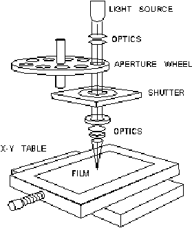
Fig 2. Laser photoplotter 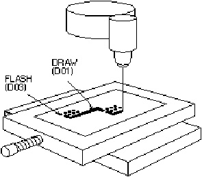
Virtually every PCB CAD system generates Gerber data because all photoplotters read it.
It is a software structure consisting of X-Y coordinates supplemented by commands that define where and when the PCB image starts, what shape it will take (which tool to use), whether to go there in a straight line or along an arc and where it ends. In addition to the coordinates, Gerber data contains aperture information, which defines the shapes and sizes of lines, holes, and other features3. The vector photoplotter has commands that control the X-Y movement of the table and film. There are also additional commands that control the rotation of the aperture wheel to align the correct shape to be exposed.
Laser plotters (Fig.2) work in a completely different way to a vector plotter. Its operation can be compared to a desktop scanner or a photocopier machine, where the process time does not depend on the number of words on the document, because the copying is performed in a single pass of the light source. The command instructions are now in a raster format of the bitmap image to simply switch laser on or off. That is, when there is a black pixel indicating a line to draw the laser switches (flashes) on. Alternatively, where there is no line to be drawn the laser turns off. Laser plotters operate much quicker than vector machines and this revolutionised the industry. A complex plot on say a 24x18 artwork that required 10 hours on a vector machine can usually be performed in ten minutes or less on a laser plotter. This decreases turnaround time and in many markets has driven down the cost of photoplotters. Today a laser plotter with a one metre diameter drum would typically cost Ł100,0001.
5. RECENT DEVELOPMENTS
With the invention of the laser photoplotter, the commands were totally different and no longer depended on Gerber data format to give instructions. Instead of NC data the commands are simply switch laser on or off in different positions for varying time periods. This meant that a lot of the constraints were lifted, and the CAD/CAM industry has seized the opportunity to develop software and design in much more flexibility. From the design process the photplotting file is created. The design data enables production of all the other data used in producing PCB’s like master artworks, silkscreen, solder mask, drill templates, shaping and profiling of the board, component placement and assembly, inspection and electrical testing. Other than Gerber, there are other formats e.g. HPGL, DXF, DWG and are listed in the accompanying PowerPoint presentation).
Gerber’s RS-274-D's data format was basically vector data, the operator of the photoplotter was required to input all the format and aperture wheel data manually. This, by its very nature, was error prone, and has now become almost obsolete and caused numerous problems.
Gerber RS-274-X was derived from 274-D. 274-X data now includes all the format information, aperture information (known as the wheel file) and micro codes used to provide intricate details for custom apertures4. However, because Gerber had such a massive stake in the market it is still by far and away the most used format.
IPC – D – 350 is a standard generated by the Institute and Packaging Electronic Circuits (IPC) to attempt to standardise the formats in America. As IPC were only a standards committee there was a distinct lack of marketing power behind this format. It was not in business’s interests to take this on board when they had a profitable system already. As there was very little financially benefit for the industry, this has not taken off.
ODB++ is designed and supported by Valor Computerised Systems Ltd and although relatively new, is becoming very popular, especially with larger PCB producers. It is one of the most intelligent formats that can capture all the CAD/CAM data. It is unique in that it can compare the production data with design standards it holds in its comprehensive database (hence ODB = Open Database).
GenCAM (developed by IPC) is a major step forward for the industry. It integrates functional descriptions for printed circuit boards and printed circuit assemblies into a single file format. In the past the customer would have to rely on a rag tag collection of file formats, e.g. Gerber files, Excellon drill files, or IPC 356 net list files. Some information, such as Bill of Materials data, was shipped in dozens of formats, each with a slightly different layout.
OrCAD is one of the most powerful, affordable and complete computer aided-design tools. Using the software, OrCAD/SDT (Schematic Design Tool), functional block diagrams or schematic flow charts can be drawn and OrCAD/PCB can generate all the different files necessary to produce a PCB.
6. CONCLUSION
The beauty of the Gerber database is its simplicity. The database had to be simple and compact because the first machines were driven by a fragile punched paper tape. The need to compress as much information as possible into as few bytes as possible explains many of the "problems" we encounter today when storage space is measured in hundreds of megabytes instead of hundreds of bytes. But simplicity exacts its own price. The Gerber file lacks essential information necessary to run the plotter. This missing data is handed from the designer to the plotter operator separately, and is often the source of errors. Further, the temptation to create non-standard extensions is impossible to resist. Every photoplotter manufacturer supports the basic Gerber commands plus whatever features they feel necessary to differentiate their machine. The result is that one man's feature is the next man's unsupported problem.
Hence, the introduction of the vast range of formats. Therefore, it is not the format type that is the over-riding factor, but the way the CAD/CAM software manages and manipulates these in the most effective way. Features to look for in a CAD/CAM software format are: that it is much better and simpler and the system defines only one file to do the job. But also, has to be able to accept other formats as input in a way that is versatile to the design and production of the company. If manufacturers want to succeed they need to follow the trend to make smaller and more technically advanced electronic products. More modern methods are being used with, more adaptable software, more accurate design and assembly of smaller, more densely mounted PCB’s. A prime example of how this has had an impact on society can be seen in the reduction in size of mobile phones and camcorders.
7. REFERENCES
1. Philips M., Director, Philips Precision Photography, Letchworth UK, 2001
2. DiBartolomeo S., Applications Manager, Artwork Conversion Software Inc.
3. Frankum C., Senior Applications Engineer, Cadence Design Systems, , 2001.
4. Carr D., President, D03* Inc & Editor, Everything PCB, 2001.
5. Coates J., Vice President, Corporate Marketing, Valor Computerised Systems Ltd, , 2001.
6. Hossain A., “Computer-Aided Electronic Circuit Board Design and Fabrication” “Using OrCAD/SDT and OrCAD/PCB Software Tools”, P.4, Prentice-Hall, 1996.
7.Toyofuko K., Interconnect Technology for Achieving Small Size Lightweight Camcorders, Surface Mount Technology, Recent Japanese Developments, P.40, 1992.
8. BIBLIOGRAPHY
Axelson J., “Making Printed Circuit Boards”, P.111,1st Edition, TAB Books, 1993.
Lindsey D., “The Design & Draughting of Printed Circuits”, P.336, 2nd Edition, Bishop Graphics, 1986.
Page T., “Electronics Manufacturing Technology”, P.59, Page T., 2001.
Scarlet J.A., “Printed Circuit Boards for Microelectronics”, P. 98, 2nd Edition, Electrochemical Publications Ltd., 1987.